Except for the concept of a machine cycle, the SFL language may appear far removed from hardware implementation. How then does it cope with the various problems encountered in actual logic circuit design, such as eliminating circuits by logic simplification, achieving high-speed by shortening the delay time of critical paths, avoiding clock hazards and skew, ensuring adequate gate drive power, and evaluating register setup time and hold time?
In PARTHENON, the information for this type of laborious work, which accounts for the major part of actual logic circuit design work, is confined to languages other than the SFL language. These are NLD and PCD. In this way, the SFL language is designed to express only the highly advanced thoughts of the user (with a high level of abstraction).
These other languages are used to express the following:
NLD: Actual circuit connection structure
PCD: Component element load capacitance, delay time, and other physical characteristics
These languages, together with the mapping & logic circuit optimization program OPT_MAP, can generate actual circuit information complying with the cell library of a specific manufacturer.
This chapter first describes the NLD and PCD languages and then goes on to explain how to express the cell library of a specific manufacturer in these languages.
NLD (Net List Description) is a netlist description language of PARTHENON. A netlist is a "list of what is connected to what."
In NLD, all connection terminals are presented in a plain list. Such a presentation is called an equipotential expression. Let's look at an example. The circuit shown in Figure 4.1 can be expressed in NLD as follows:
 1:  (def-module test
 2:      (def-pin abc type input)
 3:      (def-pin def type input)
 4:      (def-pin xyz type output)
 5:      (def-pin uvw type output)
 6:      (def-comp and--2 and-1)
 7:      (def-net abc and-1.in1)
 8:      (def-net def and-1.in2)
 9:      (def-net uvw xyz and-1.out)
10:  )
<Fig 4.1> Simple circuit example
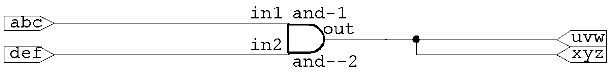
"(def-comp and --2 and-1)" in the 6th line indicates that a part by module (part type) name of "and--2" is a component element, which is used by the sub-module (intrinsic) name of "and-1."
The concepts of module and sub-module are the same as in the SFL language.
"(def-net uvw xyz and-1.out)" in the 9th line indicates external terminals "uvw" and "xyz" and terminal "out" of sub-module "and-1" are interconnected.
The NLD language is expressed in the BNF format as follows.
The full structure is as follows:
NLDescription ::=
	(def-module ModuleName
		{DefinitionOfExternalTerminal}
		{DefinitionOfComponentElement}
                {DefinitionOfNet}
	)
Only the following characters are allowed for names in the NLDescription: 'a'-'z', 'A'-'Z', '0'-'9', '_', '-', '[', and ']' (the first character is limited to 'a'-'z' or 'A'-'Z'). Note that a ModuleName must correspond to the file name (ModuleName.nld) in which an NLDescription is stored. For example, for (def-module test ....) the file name must be "test.nld." Only one module can be described in a single file.
Comments in the NLDescription are placed after ; up to the end of the line.
An external terminal of a module is defined as follows:
DefinitionOfExternalTerminal ::= (def-pin ExternalTerminalName [type TerminalType])
TerminalType  ::=
		  input
		| input-connected
		| output
		| output-connected
		| bidirect
		| bidirect-connected
		| tristate
		| tristate-connected
		| global
		| unused
		| unused-connected
This TerminalType is used to provide information to people and programs outside PARTHENON.
The following methods are used to express terminal types:
Terminal-type generation methodTerminal-type preservation method
Terminal-type generation method
The terminal-type generation method is used when the NLD file is produced by OPT_MAP with the "write" command or "last" command. All terminal types except "global" are generated from the circuit structure as shown in Table 4.1.
<Table 4.1> Terminal types generated from circuit structure
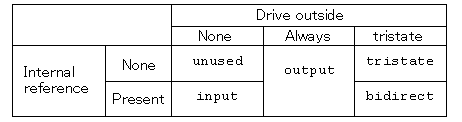
Terminal type "-connected" indicates this external terminal is connected to another external terminal. For example, "unused-connected" indicates two or more external terminals are merely connected and not used internally. The only external terminals of terminal type "global" are VDD and VSS.
In the terminal-type generation method, inputs and outputs described in SFL may become "....-connected". For example, when
module test {
    input abc ;
    output xyz;
    xyz = abc;
}
undergoes logic synthesis by means of the "write" and "last" commands of OPT_MAP, both abc and xyz become "unused-connected," resulting in no differentiation between input and output. You may think something is wrong, but the equipotential expression we adopted results in this situation. In this example, abc and xyz are equipotential and not directional.
Terminal-type preservation method
If, on the other hand, the write_org_type command or last_org_type command is used to produce an NLD file from OPT_MAP, you are using the terminal-type storage method. The external terminal of the top module preserves the terminal type from the time OPT_MAP read the input. In some cases, VDD and VSS may be added.
As far as internal modules are concerned, terminal types cannot be preserved because they undergo logic compression and thus their circuit structure may change. Instead, terminal types are generated from the circuit structure.
If an NLD is produced by SFLEXP (HSL_NLD to be exact), the terminal type used in SFL is preserved. In this NLD, terminal types are defined as follows. "unused," "tristate," "global" and "-connected" are not used. The input terminal, output terminal and bidirect terminal in SFL become input, output and bidirect, respectively.
The result of logic synthesis produced by the "auto" command using the celldemo library is based on the terminal-type preservation method.
Component elements are defined as follows:
DefinitionOfComponentElement ::= (def-comp ModuleName {Sub-moduleName})
Component elements cannot be used in the net without first being defined.
A net shows what is connected to what and is defined as follows:
DefinitionOfNet ::= (def-net {ConnectionTerminal})
ConnectionTerminal  ::= ExternalTerminalName
	    | Sub-moduleName.TerminalName
All terminals which are connected together as an equipotential net must by described in a single net statement. For example:
    (def-net a b)
    (def-net b c)
is an error. In this case, the description should be as follows:
(def-net a b c)
The PCD (Physical Characteristic Description) language expresses the lowest layer elements (cells) in a logic circuit. Let us first take a simple example. List 4.1 is a PCD description of a 2-input nand gate. The external terminal type ("type"), load capacitance ("load"), symbol shape, cell function, delay and drive capacity are defined.
<List 4.1> PCD description of 2-input nand
(def-module nand--2 power 4 area 1.10592 gates 1
        (def-pin  in1  type input  load 0.10)
        (def-pin  in2  type input  load 0.10)
        (def-pin  nout type output load 0.09)
        (def-symbol  NAND in1 in2 nout)
        (def-function  ^nout (and in1 in2))
        (def-delay  /in1 /nout (+ 0.5 (* 4.1 ~nout)))
        (def-delay  /in2 /nout (+ 0.5 (* 4.1 ~nout)))
        (def-delay  %in1 %nout (+ 0.5 (* 4.1 ~nout)))
        (def-delay  %in2 %nout (+ 0.5 (* 4.1 ~nout)))
        (def-constraint  drive (- 0 ~nout) type max)
)
The full structure is as follows:
PCDescription ::= (def-module ModuleName {Attribute} {VariousDefinition} )
VariousDefinition ::= DefinitionOfExternalTerminal | DefinitionOfSymbol | DefinitionOfFunction | DefinitionOfDelay | DefinitionOfConstraint | ...The ModuleName is a part type name in PARTHENON. In most cases, the cell name provided by the LSI manufacturer is used as a ModuleName . In some cases, however, a different name must be given. For details, see "CellName" below.Attribute ::= power Value | area Value | gates Value | cell_name CellName
Value ::= +12.333|0.23|.12|2|2e5|2E3|+.1e3|etc.
As in the NLD language, the ModuleName must correspond to the file name ( ModuleName.pcd) of the file that stores the PCDescription. Only the following characters are allowed for the various types of name used in the PCDescription: 'a' to 'z', 'A' to 'Z', '0' to '9', '_', '-', '[', and ']' (the first character is limited to 'a' to 'z' and 'A' to 'Z').
Attributes "power," "area" and "gates" denote cell power consumption, area, and equivalent number of gates, respectively. OPT_MAP is used only to total these values and display cells sorted by cell magnitude. Units of measurement need not be specified. However, when you create libraries, the same units must be used for each entry in the library. The units of measurement for power, area and gate used for cells in the celldemo library are uW/MHz, 1000 um2 and gate, respectively. Since these units of measurement are not used in circuit conversion, they do not affect the resulting circuit. The default values of these Attributes are 0.
Negative Values are not allowed. When the Values is 0, use 0, not 0.00 etc.
Comments in a PCDescription are placed after ";" and continue up to the end of the line.
The CellName is used when you want to define multiple part types (modules) for the same cell.
For example, suppose you want to use the same latch as both a master latch and a slave latch. In general, the master latch output is considered to be stable from the falling edge of the clock pulse, whereas the slave latch output is considered to be stable from the rising edge of the clock pulse, although these depend on the clock waveform supplied. Since the two types of latch have different delay expressions and constraint expressions, you must make two different modules. You make the CellName for these two modules the same as the CellName of the original latch. This differentiation must be maintained until the OPT_MAP program is terminated.
In the DefinitionOfComponentElement in the netlist (NLD file) produced with the "last" or last_org_type command in OPT_MAP, the ModuleName is the cell name in the PCD description. So no distinction is made in the later processes. This NLD file must not be read into OPT_MAP again to modify the circuit further. This is why the command name is called "last."
On the other hand, in the DefinitionOfComponentElement in an NLD file produced with the "write" or write_org_type command, the ModuleName is the ModuleName of the PCDescription. In this case, the above distinction remains effective, and the NLD file can be read into OPT_MAP again for further modifying of the circuit.
If the specification of cell name is omitted, the Cellname is taken as the same as the ModuleName.
VariousDefinitions take the following format.
(KeyWord .....)
Each program that reads a PCD file is designed to skip the key words it does not require when reading a file. Table 4.2 lists the relationships between key words currently used in each type of VariousDefinitions and programs that use them.
<Table 4.2> Various definitions and programs that use them
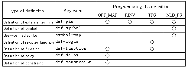 Notes: TPG is a program included only in the PARTHENON workstation version. Symbol-map and def-logic are not described in this document.
The DefinitionOfExternalTerminal is as follows.
DefinitionOfExternalTerminal ::= (def-pin external terminal name {TerminalAttribute })
TerminalAttribute ::= load LoadExpression | type TerminalType | note Note"load" is the load capacitance of this terminal alone and the default value is 0. "type" cannot be omitted. If "note" is omitted, it is assumed to be undefined. As is the case for "power", "area" and "gates", "load" does not require a unit of measurement, but it is necessary to use the same unit of measurement for all entries when making a library.LoadExpression ::= (+ {LoadExpression1 }) | LoadExpression1
LoadExpression1 ::= (* Value [LoadExpression2 ]) | LoadExpression2
LoadExpression2 ::= Value |Variable
TerminalType ::= input | output | bidirect | tristate | unused
Note ::= clock | scan_in | scan_enb | scan_out
The unit of measurement for "load" in the celldemo library cell is "pF".
Variable denotes an external variable whose value is set later. For example, you can introduce a variable indicating temperature with ?temperature and makes the load capacitance dependent on temperature. The value of ?temperature is set when a circuit is operated on by OPT_MAP.
"unused" in TerminalType denotes that it exists but is not used as a terminal. "bidirect" denotes not only that the terminal has a 3-state output but also that the signal is bidirectional. The TerminalType thus indicates the electrical characteristics of the terminal and the signal direction.
The clock attribute specified by "note" indicates that a "hazard does not occur or must not occur." For example, the "clock" attribute must be specified for a terminal that receives timing-determining signals, such as a clock input to a register. The "clock" attribute is valid only for input terminals.
OPT_MAP verifies whether the clock attribute conditions are satisfied using, as the criteria, the following condition for the arrival of a clock pulse:
"The network structure is such that no indeterminate event arises; and one rising event and one falling event arrive during each clock cycle."
If this condition is not satisfied, you cannot operate on circuits with OPT_MAP.
Note: Attributes, scan_in, scan_enb and scan_out, are used only by the test pattern creation program included in the PARTHENON workstation version. They are not described in this document.
Symbols are defined as follows.
DefinitionOfSymbol ::= (def-symbol Symbol TerminalList)
Symbol ::= AND|NAND|OR|NOR|EXOR|NEXOR|INVERTER|BUFFER |TRI_STATE|TRI_STATE1|TRI_STATE2|TRI_STATE3|REGISTER |AOI21|AOI211|AOI22|AOI221|AOI222|AOI31|AOI32|AOI33 |OAI21|OAI211|OAI22|OAI221|OAI222|OAI31|OAI32 |OAI33The DefinitionOfSymbol is used only when creating a circuit diagram with NLD_PS and does not affect circuit synthesis.TerminalList ::= {InputTerminalName} {OutputTerminalName}
The Symbol indicates the shape of a module (part type) in a circuit diagram. TRI_STATE1, TRI_STATE2 and TRI_STATE3 indicate, respectively, reverse output, reverse control input (the module is driven if the control input is '0'), and both output and control input being reversed. AOI is a composite gate of the form "and-or-inv," and OAI is a composite gate of the form "or-and-inv." You should be able to infer the meaning of the names of these composite gates from the following:
AOI32: (INV (OR (AND in1 in2 in3) (AND in4 in5)))
AOI211: (INV (OR (AND in1 in2) in3 in4))
The names and types in the TerminalList must be consistent with those in the definition of the external terminals. In a circuit diagram, the input terminals and output terminals are placed to the left and right of a symbol, respectively. Both input terminals and output terminals are placed from the top of the diagram in the order they appear in the terminal list. "bidirect" and "tristate" are treated as output terminals.
OPT_MAP converts a circuit consisting of only logical cells produced by SFLEXP into a physical circuit, consisting of only real cells, which operates correctly because any violations of various physical constraints have been resolved. During this process, OPT_MAP learns the logic functions of cells from the DefinitionOfFunction and modifies the circuit without changing the meaning of the logic. DefinitionOfFunction is as follows.
DefinitionOfFunction ::= (def-function Output FunctionExpression)
Output ::= OutputTerminalName | ^OutputTerminalName^ denotes "not." ^ and the following Operators are reserved words with their meanings built into OPT_MAP.FunctionExpression ::= (Operator {FunctionExpression}) | Input
Input ::= InputTerminalName | ^InputTerminalName
	(and f1 f2 ...)
	(or f1  f2 ...)
	(eor f1 f2 ...)
	(buffer f1)
	(clock_buf f1)
	(true)
OPT_MAP understands the meanings of these words and changes the circuit while sometimes executing logic compression (however, logic compression is not applied to clock_buf). "true" is "always true" and used to express either constant "1" or constant "0".
Even if the meaning of an Operator is not built in, OPT_MAP assumes it to be logically equivalent to an operator, if any, with the same function expression and corresponding terminals. OPT_MAP then replaces the operator with the corresponding one if required by the physical condition. This is called replacement by pattern matching.
UnreservedOperators and FunctionExpressions must represent qualitative characteristics of the module, such as ways of defining set-up time and hold time, and propagation path with significant delay.
If there are two or more ways of using the same cell, the cell must be defined as two different modules as mentioned above. All such differences in use must be included in the Operator and FunctionExpressionss.
A MduleName can be said to be a name specifying a CellName and how it is used. If every cell is used in two different ways, the number of ModuleName is twice the number of CellName.
Because of the way OPT_MAP operates, there are the following constraints. If there are several ways of expressing a function, only one form of expression should be used. If an unreserved Operator is used, FunctionExpressions cannot be nested.
DefinitionOfDelay defines how an event (change) propagates from an input terminal to an output terminal in a module. OPT_MAP determines whether there is a timing problem from this information and the information on the connections between modules. Delay is defined as follows:
DefinitionOfDelay ::= (def-delay Start End DelayExpression)
Start ::= EventThis format indicates that delay from Start to End is what is described in the DelayExpression . The DelayExpression cannot take a negative Value.Event ::= /TerminalName /* Note: in the case of rising event */ | \TerminalName /* Note: in the case of falling event */ | %TerminalName /* Note: indeterminate (high impedance) event */
DelayExpression ::= (+ {DelayExpression1}) | DelayExpression1
DelayExpression1 ::= (* Value [DelayExpression2]) | DelayExpression2
DelayExpression2 ::= TerminalLoad | Variable | Value
TerminalLoad ::= ~TerminalName
The rising and falling events include the changes from high impedance to "H" level and from high impedance to "L" level, respectively. They also indicate changes in the electrical potential of a terminal irrespective of the DefinitionOfFunction . Inconsistency with DefinitionOfFunction is not verified.
In the DelayExpression , "+" denotes addition. For example, (+ 2 3 4) is 9. If there are no elements is to be added, as in (+ ), the result is 0. In DelayExpression1 , "*" denotes multiplication. For example, (* 2 4 3) is 24. If the number of elements to be multiplied is 1, as in (* 3.0), the result is 0.
TerminalLoad (i.e., ~TerminalName) denotes the total load applied to the terminal (including the load of the terminal itself). Therefore, the value of the load cannot be determined until after the netlist has been read.
As explained before, for a terminal with a "clock" attribute,
"the network structure is such that no indeterminate event arises; and one rising event and one falling event arrive during each clock cycle."
Therefore its value can only change in one of the following ways:
In the case of a terminal without the "clock" attribute, on the other hand, the value may change as follows: (KDF I am having to guess here. The original is not very easy to follow. I have tried to make it clearer, but of course what I have put may not be accurate.)
In general, for clock terminals such as a register, the waveform is important, while for data terminals, it is the value at the time of clock arrival that is important. Therefore, a clock attribute is specified for clock terminals but not for data terminals.
In addition, in a delay path with a clock attribute, the rising event and falling event at each terminal must be clearly distinguished. However, in a delay path without a clock attribute such distinction is not necessary, so a rising event can be made to "represent both a rising event and a falling event" in order to speed up delay evaluation or to simplify cell library creation (although such simplification compromises accuracy to some extent).
The unit of measurement used in the celldemo library is "ns". An example of DefinitionOfDelay is given below.
(def-delay /a1 /zn (+ 0.5 (* 4.1 ~zn)))
This example indicates that "the elapsed time between the time when a rising event was applied to input terminal "a1" and the time when a rising event is witnessed at output terminal "zn" as a result is given by the sum of a fixed time of 0.5 (ns) and a value proportional to the load capacitance on the net connected to output terminal "zn," and that the constant of proportionality is 4.1 (ns/pF)."
The DefinitionOfConstraint indicates conditions to be satisfied. OPT_MAP uses this information to determine whether a circuit is physically correct, and if not, to amend the circuit as necessary. OPT_MAP handles virtual cells and real cells in the same way. Virtual cell are converted into real cells because virtual cells may contain constraints that cannot be satisfied.
The DefinitionOfConstraint is given in the following format.
DefinitionOfConstraint ::= (def-constraint constraint name ConstraintExpression [type ConstraintType])
ConstraintExpression  ::=  (- {ConstraintExpression1})
	    | ConstraintExpression1

ConstraintExpression1  ::= (+ {ConstraintExpression2})
	    | ConstraintExpression2

ConstraintExpression2  ::= (* Value [ConstraintExpression3])
	    | ConstraintExpression3

ConstraintExpression3 ::= TerminalLoad
	    | Event
	    | Variable
	    | Value

ConstraintType  ::= ConstraintTypeName
That the value of a ConstraintExpression should never take a negative value even in the worst case is the requirement. The constraint name is an arbitrary name defined by the user and is used by OPT_MAP to indicate the state. The constraint name cannot be the same as a terminal name.
In the ConstraintExpression, "-" denotes difference.
(- a b c ...)
denotes that the values of the second and subsequent elements are subtracted from the value of the first element. For example, (- 10 2 3) denotes 10-2-3=5, (-5) denotes 5-0=5, and (-) means 0-0=0.
The ConstraintExpression3 for an event denotes the event's value (time). This value changes depending on where the PCD module with this constraint is located in the circuit. Generally, two or more events may arrive at a terminal without a clock attribute. If several events arrive, OPT_MAP pays attention to the earliest and the latest. The constraint evaluation selects an event that minimizes the value of the expression.
For specific ConstraintTypes, OPT_MAP changes circuits as given in Table 4.3.
<Table 4.3> Constraint types and changes in circuits
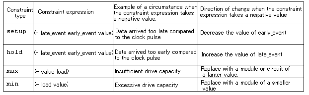
If a ConstraintType is not specified, a constraint error is reported and no circuit optimization is performed.
Example of definition of constraint
As an example of DefinitionOfConstraint, let's describe the setup time and hold time of an edge trigger type register in PCD.
<Fig 4.2> Constraint on setup time and hold time of a register
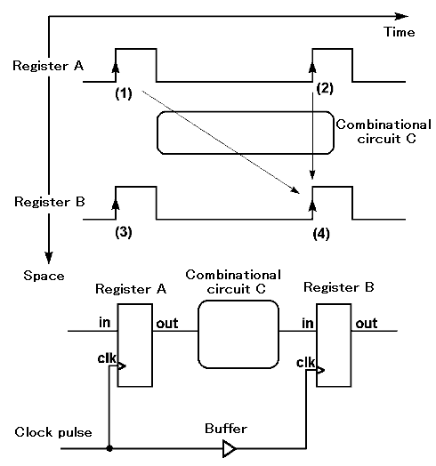
As shown in Figure 4.2, the content of register A is processed in combinational circuit C and the result is written into register B.
The output of register A is updated on the arrival of clock pulse (1). This change propagates through combinational circuit C and arrives at the input of register B. If the time from the arrival of the latest change in signal (KDF 1)at register B to the arrival of clock pulse (4) is greater than the setup time, the requirement for setup time is satisfied.
On the other hand, the output of the register is further updated by clock pulse (2), and that change also propagates through combinational circuit C to arrive at the input of register B. If the earliest event arrives within the hold time of clock pulse (4), the hold time requirement is not satisfied and writing into register B is not carried out correctly. The hold time requirement applies not only to propagation from (2) to (4) but also to that from (1) to (3).
Since events (1) and (2) and events (3) and (4) are all rising events for clock terminals clk of registers A and B, these events become "/clk" and, therefore, cannot be differentiated. To avoid this situation, if there are cyclic events, only one of them is described by "/clk." Suppose in this example that event (1) or event (3) is described by "/clk." If an external variable ?cycle is introduced, the time of (2) or (4) becomes "/clk + ?cycle" (the name of the variable is arbitrary; it is the person who described the PCD that knows that this variable indicates a cycle). "+ ?cycle" indicates the next something.
The above discussion assumes that clock pulses are distributed to all registers through only buffers, in such a way that the events driven by the present clock pulse and the events driven by the next clock pulse can be easily distinguished.
If this is so, the setup time requirement at time (4) becomes
(def-constraint setup (- (+ /clk ?cycle) /in 4) type setup)
where 4 is the setup time. Although any unit of time may be employed, the same unit must be used consistently. This requirement means
(/clk + ?cycle) - /in > 4
Thus, "the arrival time of the next clock pulse must be at least 4 units of time later than the last event for "in" due to the previous clock pulse." In other words, if the unit of time is "ns", the last event for "in" arrives at least 4 ns earlier than the next clock pulse. The reason why the arrival time of the last event is evaluated is that an event that minimizes the constraint expression value is selected as described above.
The hold time requirement in (3) is
(def-constraint hold (- /in /clk 2) type hold)
where 2 is the hold time. This requirement means
/in - /clk > 2
This denotes that the arrival time of the first event for "in" must be later by at least 2 units than the arrival time of the clock pulse. In other words, if the unit of time is "ns," it denotes that the earliest event for "in" arrives at least 2 ns later than the present clock pulse.
The operation of the hardware described in SFL is converted into a circuit consisting of logical cells and dummy cells for optimization before it is finally converted into a circuit consisting of real cells.
Real cells
Real cells are existing (manufacturable) component elements. The cell names, terminal names, functions, etc. are as specified by the manufacturer or by the product line.
Virtual cells
(1) Logical cells
For a logical cell, the cell name, terminal name, function, etc. are defined in PARTHENON (physical information, such as terminal load capacitance, drive capacity and delay time, is excluded). The SFLEXP, RINV and ONSET programs handle a circuit taking the presence of logical cells and their meanings for granted.
(2) Dummy cells
The dummy cell serves as an intermediary between logic and real cells. When a cell library is created, the cell name, terminal name, function, etc. are determined such that a logical cell can be correctly converted to a real cell.
Logical cells, dummy cells and temporary non-inverters described later are called virtual cells. Figure 4.3 shows the relationship between virtual and real cells.
<Fig.4.3> Cell library types and their relationship to each other
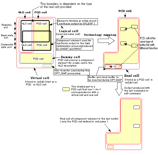
PCD cells and NLD cells
In addition to the above classifications, cells can be classified according to the description language used. Cells defined in PCD and NLD are called PCD cells and NLD cells, respectively.
If, for example, there is no real cell that corresponds to a logical cell, an appropriate real cell is selected and a dummy cell is defined with the same function as the selected real cell. A logical cell without a corresponding real cell is defined as an NLD cell using this dummy cell and a logical cell that does have a corresponding real cell.
The flip-flop that constitutes a register should not be configured as individual gates, but only used as a pre-defined module.
Procedures up to real cell mapping
While the compressed result must be mapped onto real cells with as many functions in it as possible, the current processing is restricted to the following phases performed in sequence.
Mechanism of real cell mapping
To create a cell library correctly you must fully understand each phase. See Figure 4.4. The path on the left side of the figure is for circuit parts (combinational logic circuit parts) consisting of PCD cells whose functions are defined by "and", "or", "not" and "eor". The path on the right (control circuit part, etc.) is for PCD cells representing registers and clock gates ("and" circuits determining whether or not a clock pulse is passed).
In phase1 and phase2 in the chart, the right side is not affected except for deletion of clearly unnecessary portions. In contrast, on the left side, circuits are compressed and some parts are replaced with logical cells which incorporate as many functions as possible. In phase3, PCD logic or dummy cells are converted to real cells having the same function definitions.
<Fig. 4.4> Mechanism of real cell mapping
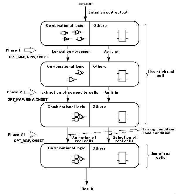
The mechanism in phase3 indicates that "logical cells and PCD dummy cells not corresponding to real cells must not be included in a library."
Mappable cells
On the left side, the mapping to sophisticated (meaning incorporating many functions) physical cells is determined by the logical cell extraction in phase2. On the right side, it is determined by the logical cells in the initial circuit. However, on the right side, the mapping should be limited to extremely sophisticated cells whose use would make up for the drawback of absence of logic compression. Logical cells of an initial circuit as well as logical cells extractable in phase 2 are shown in Table 4.4 at the end of this chapter.
Refer to the table in the following example.
Suppose there is a real cell corresponding to a logical cell of the type "4-bit 2-input selector." On which side of the mapping mechanism should it be processed. First, we confirm that such a selector is listed in Table 4.4 and named "sl4-2." Since "s14-2" is not the kind of logical cell which can be extracted in phase 2, processing by the left-side route would not select the real 4-bit 2-input selector cell. On the other hand, the processing by the right-side route would indeed allow it to be selected and used in the final result but no circuit compression takes place. So, which is preferable depends on the individual case.
The policy of using the left-hand processing as much as possible is not problematic. In either case, a cell library has to be created so that the logical cells included in the initial circuit produced by SFLEXP can be converted into real cells through either the right-side path all the way or the left-side path all the way.
Two "nand" gates
Although logical cells "bgate--2" and "nand--2" are physically the same 2-input "nand" gates, they must be differentiated in the logic synthesis of PARTHENON. That is,
In phase3 in Figure 4.4, a satisfactory constraint mechanism is used to convert logical cells and dummy cells into real cells. Therefore, the closer the physical information, such as the terminal capacity, delay time (excluding load drive capacity), of both the logic or dummy cell and the real cell, the better the result.
A PCD logic or dummy cell should have an output terminal drive capacity of 0 so that it will be converted to a real cell.
Handling of non-inverter, buffer, and clock buffer
The processing in phase1 temporarily requires a non-inverter whose function is defined by
(def-function out in)
This is treated as a virtual cell.
Some real cells are not associated with logical cells. They are buffers and clock buffers. Their functions must be defined by
(def-function out (buffer in))
(def-function out (clock_buf in))
Some product series physically differentiate non-inverters, buffers, and clock buffers, and some do not. Even if a product series does not differentiate them, they must be treated as different real cells in the logic synthesis of PARTHENON. In this case, the original name is defined for cell_name.
Use of "auto" command
If the "auto" command is used, the following must be stored in respective directories:
What kind of dummy cells are required and how a logical cell is expressed depend on the characteristics of real cells. Therefore, a virtual cell must be provided for each real cell.
When you wish to create a new cell library, please first make sure that you understand the cell library example in the "celldemo" directory.
Table 4.4 lists logical cells. Some logical cells are used in the initial circuits mentioned earlier. Others are used in the extraction of highly complex cells with sophisticated functions.
The table also includes non-inverters, which are used temporarily during the logic compression process in phase 1, and buffers and clock buffers, which are used to satisfy constraint in phase 3, although they are not strictly logical cells.
In addition, some logical cells in the initial circuit can be disassembled into a netlist showing connections between other logical cells, and others cannot. In Table 4.4, ¤ indicates a logical cell that can be disassembled. Disassembly can be specified by attaching the "-nld" option (default is disassembled) when activating SFLEXP.
<Table 4.4> List of logical cells
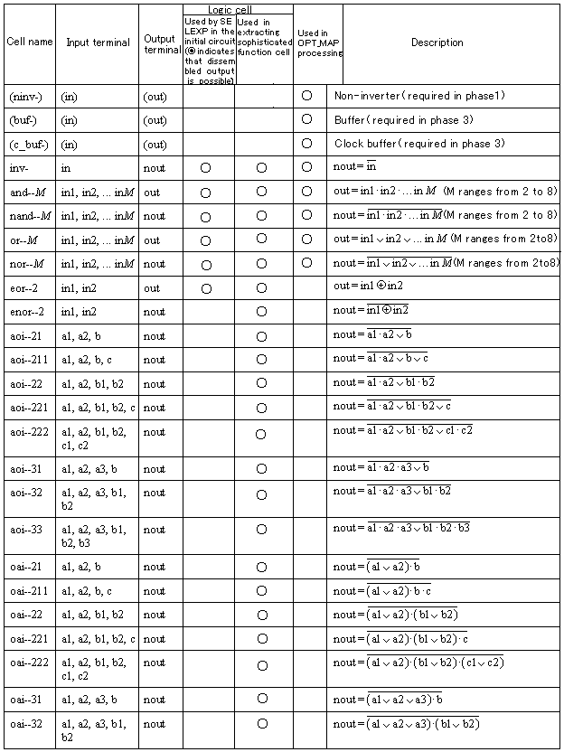
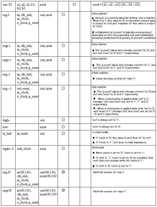
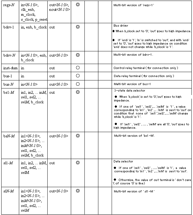
Notes: o The register "clk_enb" signal can be configured to control clock pulses or to control data as a free-running clock (continuously supplying clock pulses).
M denotes the number of fan-ins or the number of selections.
N denotes the number of bits.
o In NLD, "a