• Basic functions of OPT_MAP
Mapping & logic circuit optimization program OPT_MAP (OPTimizer and technology MAPper) uses the following as inputs:
OPT_MAP automatically carries out its primary function of optimization in such a way as to satisfy the design requirements and the constraints of each component element. During this process, technology-specific mapping is also carried out, (that is matching the design to the particular technology in which it is proposed to build the physical circuit).
In addition, OPT_MAP provides miscellaneous other functions: control of the hierarchical structure, replacement of portions of the circuit, removal of redundant parts of the circuit, and verification of various physical characteristics (delay time, load capacitance, area, etc.). The operation of these functions is controlled by commands given to OPT_MAP.
• NLD module and PCD module
While only a single component element exists for each class (type) in the NLD and PCD files, all the component elements corresponding to different instances (entities) as well as hierarchical and connection relationships between them are constructed in the model in computer memory.
Among the component elements incorporated in the model for internal processing of OPT_MAP, are the following:
• Format of start command
OPT_MAP searches the directory given in the start command and attempts to construct internally a circuit under the specified top module name. If the circuit cannot be constructed because "required files for component elements are not found," "the specified directory does not exist" or "the format of either the PCD file or NLD file is erroneous," the operation is immediately aborted.
OPT_MAP starts by reading the required NLD and PCD files in the following order.
When the circuit has been successfully constructed and all initial operations for OPT_MAP are complete, the following prompt is displayed:
OPT_MAP>
The system is now ready for command entry from a standard input (e.g. a file). During the subsequent interactive processing, various messages are output to a standard output. OPT_MAP commands are outlined in Section 7.5. For an explanation of command functions, use the help command.
• Examples of starting OPT_MAP
In the following example, OPT_MAP is started using the netlist in sub-directory 'TIMER.1st' and a virtual cell library in 'A:\par\celldemo\start' (see the explanation on cell libraries in Section 4.3) to construct a circuit with top module name 'TIMER'.
• Usage in auto.bat
As shown in an example in Section 2.3, OPT_MAP is activated twice during logic synthesis initiated by auto.bat. For the two activations, OPT_MAP carries out the following operations according to the script file given. This is an example of a typical use of OPT_MAP.
When OPT_MAP is activated for the first time, it does the following, in order to logically (i.e., in a manner which is technology-independent) simplify the circuit consisting of PCD modules taken from the virtual cell library.
After the execution of RINV, OPT_MAP is activated for the second time to do the following, in order to perform technology mapping and optimization in such a way as to satisfy the constraints:
When OPT_MAP is activated by auto.bat for the second time, design conditions are set using the set and max commands in preparation for optimization. However, if auto.bat is executed normally, a script file by the name of module_name.op2 is created from template file opt_scr.op2 which existed in the directory where the cell library is. Thus, the values set in this template file are used as they are. If you use 'celldemo' attached to PARTHENON as the cell library, you may find the design conditions set there too loose and unrealistic.
To ensure correct optimization, you can change script file 'module_name.op2' using an editor, so that the design conditions reflect actual working conditions. Then re-execute OPT_MAP with auto.bat.
• Further advanced usage
Circuit size, hierarchical structure, logic characteristics of sub-modules, unique features of the cell library components, design conditions, etc. vary greatly depending on the design target. All logic synthesis can be performed by auto.bat. However, applying the same procedure to all design targets is not maximizing PARTHENON's logic synthesis capability.
Therefore, to benefit fully from the capability of OPT_MAP or ONSET, you should proceed interactively, using the OPT_MAP command interface, considering the circuit characteristics and the extent of optimization. To do so, you need to fully understand the OPT_MAP functions.
• Hierarchical structure and commands
OPT_MAP provides a command interface that shows the sub-module hierarchical structure in the same way as the hierarchical directory structure of UNIX or MS-DOS. That is, as with the 'cd' command in UNIX, you can move the current module with the 'move' command, and you can display information only within a module.
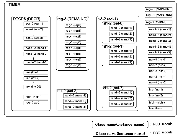
List 7.1 shows a command execution example for reading the netlist from TIMER.1st in the example provided in Section 2.3. You will see that the hierarchical structure shown in Figure 7.1 is created from these commands.
<List 7.1> Example of viewing information on the hierarchical structure of the initial circuit
 1:  A>opt_map TIMER TIMER.1st a:\par\celldemo\start
 2:
 3:  ***************************************************************
 4:  * OPT_MAP  Version 2.3.0                           1994/07/05 *
 5:  * This program is a part of the PARTHENON system.             *
 6:  *                                 Copyright (C) 1989-1994 NTT *
 7:  ***************************************************************
 8:
 9:  ** load library from TIMER.1st **
10:  ** load library from a:\par\celldemo\start **
11:  opt_map: start to read AND--2.PCD
12:  opt_map: start to read AND--3.PCD
13:  ------------------ (omission) ---------------------
14:  opt_map: start to read TIMER.1st/reg-8.nld
15:  opt_map: start to read TIMER.1st/sl1-2.nld
16:  OPT_MAP> move
17:          position   = /
18:          type       = NLD
19:          class_name = TIMER
20:          power      = 503.6
21:          area       = 72.6
22:          gates      = 264
23:  OPT_MAP> lsn
24:  type class  power         area                 gates  sub_mod_name
25:  ------------------------------------------------------------------
26:  nld  sl1-2  1.020000e+01  1.470000e+00             6  sel-2
27:  nld  reg-8  1.440000e+02  2.400000e+01            80  REMAINED
28:  nld  DECR8  1.284000e+02  1.722000e+01            64  DECR
29:  nld  sl8-2  8.160000e+01  1.176000e+01            48  sel-1
30:  OPT_MAP> move REMAINED
31:  OPT_MAP> lc
32:  type nof_instances  sum_of_power   sum_of_area  sum_of_gates  class_name
33:  ------------------------------------------------------------------------
34:  pcd              8  1.440000e+02  2.400000e+01            80  reg-1
35:  OPT_MAP> ls
36:  type class  power         area                 gates  sub_mod_name
37:  ------------------------------------------------------------------
38:  pcd  reg-1  1.800000e+01  3.000000e+00            10  reg0
39:  pcd  reg-1  1.800000e+01  3.000000e+00            10  reg1
40:  pcd  reg-1  1.800000e+01  3.000000e+00            10  reg2
41:  pcd  reg-1  1.800000e+01  3.000000e+00            10  reg3
42:  pcd  reg-1  1.800000e+01  3.000000e+00            10  reg4
43:  pcd  reg-1  1.800000e+01  3.000000e+00            10  reg5
44:  pcd  reg-1  1.800000e+01  3.000000e+00            10  reg6
45:  pcd  reg-1  1.800000e+01  3.000000e+00            10  reg7
46:  OPT_MAP> move ../DECR
47:  OPT_MAP> lc
48:  type nof_instances  sum_of_power   sum_of_area  sum_of_gates  class_name
49:  ------------------------------------------------------------------------
50:  pcd              8  8.000000e+01  6.880000e+00            32  eor--2
51:  pcd              1  0.000000e+00  0.000000e+00             0  high-
52:  pcd             20  2.800000e+01  7.400000e+00            20  inv-
53:  pcd              1  0.000000e+00  0.000000e+00             0  low-
54:  pcd              6  2.040000e+01  2.940000e+00            12  nand--2
55:  OPT_MAP> move ../sel-1
56:  OPT_MAP> ls
57:  type class  power         area                 gates  sub_mod_name
58:  ------------------------------------------------------------------
59:  nld  sl1-2  1.020000e+01  1.470000e+00             6  sel-0
60:  nld  sl1-2  1.020000e+01  1.470000e+00             6  sel-1
61:  nld  sl1-2  1.020000e+01  1.470000e+00             6  sel-2
62:  nld  sl1-2  1.020000e+01  1.470000e+00             6  sel-3
63:  nld  sl1-2  1.020000e+01  1.470000e+00             6  sel-4
64:  nld  sl1-2  1.020000e+01  1.470000e+00             6  sel-5
65:  nld  sl1-2  1.020000e+01  1.470000e+00             6  sel-6
66:  nld  sl1-2  1.020000e+01  1.470000e+00             6  sel-7
67:  OPT_MAP> move sel-0
68:  OPT_MAP> ls
69:  type class    power         area                 gates  sub_mod_name
70:  --------------------------------------------------------------------
71:  pcd  nand--2  3.400000e+00  4.900000e-01             2  nand-3
72:  pcd  nand--2  3.400000e+00  4.900000e-01             2  nand-2
73:  pcd  nand--2  3.400000e+00  4.900000e-01             2  nand-1
74:  OPT_MAP> move /
75:  OPT_MAP> lc
76:  type nof_instances  sum_of_power   sum_of_area  sum_of_gates  class_name
77:  ------------------------------------------------------------------------
78:  nld              1  1.284000e+02  1.722000e+01            64  DECR8
79:  nld              1  1.440000e+02  2.400000e+01            80  reg-8
80:  nld              1  1.020000e+01  1.470000e+00             6  sl1-2
81:  nld              1  8.160000e+01  1.176000e+01            48  sl8-2
82:  pcd              1  0.000000e+00  0.000000e+00             0  high-
83:  pcd              2  2.800000e+00  7.400000e-01             2  inv-
84:  pcd              1  0.000000e+00  0.000000e+00             0  low-
85:  pcd              4  1.360000e+01  1.960000e+00             8  nand--2
86:  pcd              1  4.900000e+00  7.400000e-01             3  nand--3
87:  pcd              3  1.410000e+01  1.830000e+00             6  nor--2
88:  pcd              1  1.100000e+01  9.800000e-01             4  nor--4
89:  pcd              1  2.900000e+01  2.100000e+00             9  nor--8
90:  pcd              2  4.600000e+01  6.800000e+00            24  reg---1
91:  pcd              1  1.800000e+01  3.000000e+00            10  reg--1
92:  OPT_MAP> ls reg---1
93:  type class    power         area                 gates  sub_mod_name
94:  --------------------------------------------------------------------
95:  pcd  reg---1  2.300000e+01  3.400000e+00            12  MAIN--all
96:  pcd  reg---1  2.300000e+01  3.400000e+00            12  MAIN-RUN
97:  OPT_MAP>
<Fig. 7.1> Hierarchical structure of the initial circuit to be constructed from the NLD file in TIMER.1st
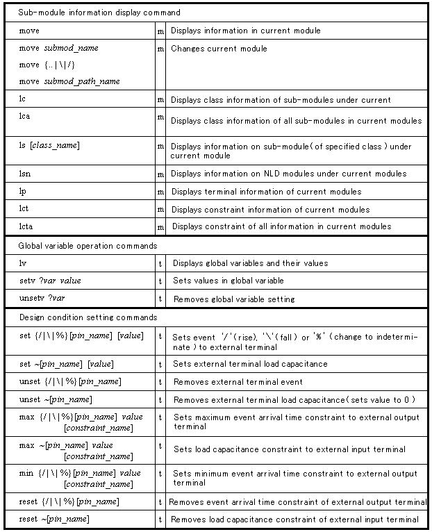
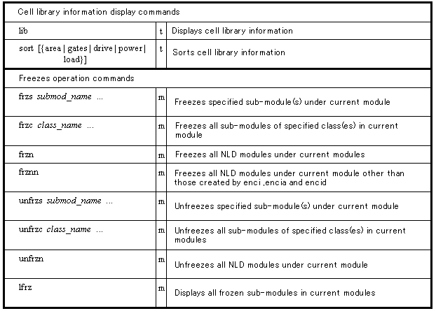
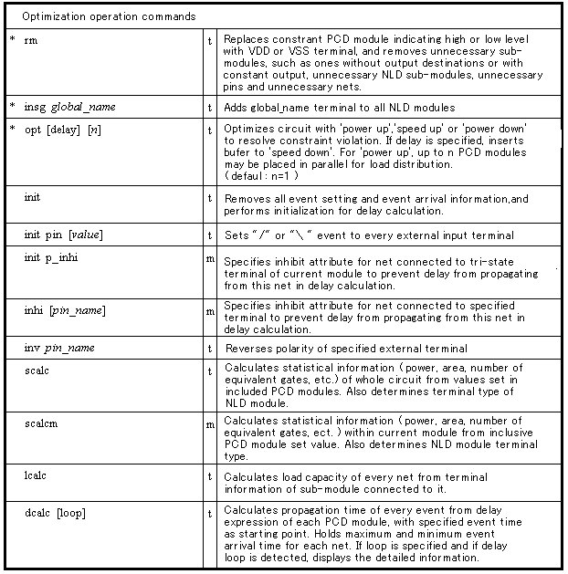
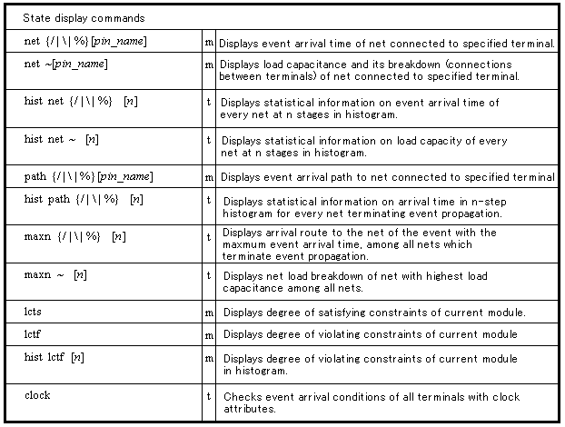
OPT_MAP commands can be classified into the following types according to their functions:
The hierarchical structure is expressed by giving containment relations to NLD modules. However, if you are only concerned about the actual operation of the whole circuit, only the top module matters. The essence of the circuit is primarily determined by the PCD modules and their interconnections. Therefore the containment relations between NLD modules, i.e., the hierarchical structure, can be changed arbitrarily without affecting the logical and physical characteristics of the whole circuit. Commands for controlling the hierarchical structure are provided for this purpose, and include the 'flat', 'make', 'encc' and 'disc' commands. The results of these commands are used in the processes after OPT_MAP, such as placement and routing.
Hierarchical structure control commands can also be used to extract a partial circuit so that it can be processed by ONSET externally and then brought it back to the original circuit. In such a case, the applicable portion is temporarily enclosed into an NLD module using the 'encia' command, i.e., a layer is generated for temporary use only.
In the course of processing by auto.bat, as shown in Section 7.3, the 'flat' command was used several times. It was necessary to flatten the hierarchical structure of the design to get around the problems arising from certain restrictions in the MS-DOS file system. Since the PARTHENON workstation version does not suffer from such restrictions, the design hierarchy can be retained up to the final netlist, and the hierarchical structure can be changed freely.
If you really want to retain the hierarchical structure even in MS-DOS, execute OPT_MAP only once (do not use RINV, and so you will not need an NLD file as an intermediate netlist) and output the final netlist only in the EDIF format.
• Removal of redundant circuits
The circuits synthesized by SFLEXP often contain clearly redundant or unnecessary circuits on the assumption that they will be removed by OPT_MAP. Therefore it is essential to use this removal function in OPT_MAP processing. The rm command starts this function, which includes the following operations:
• Defining design conditions
Listed below are the types of design condition that must be set at the external terminals of the top module, and the commands used for setting these conditions.
In each PCD file in the cell library, the conditions for normal operation of the cell are defined in the def-constraint statement (see Section 4.2). In building a circuit, OPT_MAP assumes that these conditions are the constraints of the corresponding PCD module. The only constraints used by OPT_MAP are these constraints for PCD modules, as well as the constraints for external terminals described in items (1) and (4) above.
• Evaluation of design conditions
The 'decalc' command initiates delay calculation for all events spanning the whole circuit, taking events set at the external input terminal in item (2) above as the starting point (if multiple events of the same type are set at the same terminal, each event is effective). However, the meaningful event arrival time values are the max/min times of all the "/", "\" and "%" events in each net. Delay routes not included in the above are excluded from the calculation in order to speed up the delay calculation.
<Fig.7.2> Example of OPT_MAP design condition setting and evaluation model
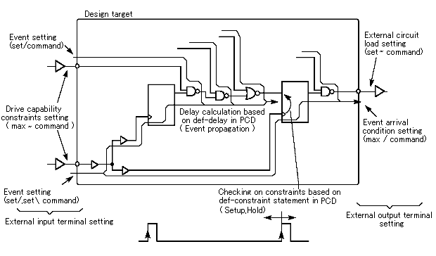
Delay propagation and time calculation is strictly based on the 'def-delay' definition in the PCD file. Therefore in considering signal propagation of a data system, whether the difference in delay time between rise and fall should be considered should be consistent between the description in the 'def-delay' statement in the cell library and the design conditions set for OPT_MAP.
The attached cell library 'celldemo' is based on a model in which data signal delay is evaluated in terms of the propagation of rising events. The def-delay statement here assumes the propagation of an event from "/" to "/" even if the logic polarity is reversed. However, "/" and "\" are distinguished in the case of clock signals.
Figure 7.2 shows an example of design condition setting and an evaluation model in OPT_MAP. The cell library assumed in this model is 'celldemo'.
The OPT_MAP setv command is used to assign values to these variables. As illustrated above, the cell library description includes important variables that can be set at execution. Therefore, it is important to assign values to these variables before starting optimization with the 'opt' command.
Although only '?cycle' is used in 'celldemo', other variables can be used to increase flexibility in setting conditions. For example, you can create a cell library in which variables are used in defining load expressions in the def-pin statement so that you can change the routing delay and evaluate its effect on the overall delay.
In fact, virtual and real cells are not implicitly differentiated in the PCD file description. A PCD module with a constraint of zero maximum load drive capacitance always triggers constraint violation, causing it to be replaced with another PCD module. As a result it is considered a virtual cell. The rule that virtual cells should be set in the "start" directory is established only for the convenience of auto.bat. This replacement mechanism forms part of the technology mapping.
In consequence, an accurate cell library and accurate design conditions are prerequisites for accurate technology mapping and optimization. This might appear to be a lot of trouble, but it is not. The PCD sub-module constraints directly reflect the constraints described in the def-constraint statement of the PCD file in the cell library. Therefore, you only need to set top module external terminal constraints carefully for each target circuit. So, even if you are dealing with a circuit containing many PCD modules in an extremely complicated hierarchical structure, the labor and time you need to spend are almost no greater than those for a small circuit.
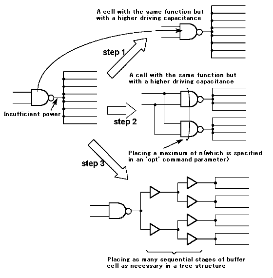
(1) power up (Fig. 7.3)
<Fig. 7.3> Example of power up with the 'opt' command
(2) speed up
If there are replaceablecells among the PCD modules in the event arrival route and if replacing them would make improvement, they are replaced in the order of the degree of expected improvement until the constraints are satisfied.
If no further improvement can be made to satisfy the constraints, a message is displayed to that effect. In such a case, improvement must be made by using ONSET, redefining the design constraints or redesigning the circuit.
(3) speed down
This improvement request often arises from errors in event values. Therefore, it is not always advisable to increase delay by inserting buffers automatically from the beginning of the operation. Because of this, if the 'opt' command has been used without a delay being specified only a warning message is displayed.
If this command is executed with 'opt delay' specified, the event arrival time is delayed by inserting as many buffers in series as necessary before output terminals of the PCD module which outputs to the last net in the event arrival route, or before the top module's input terminals.
To insert buffers, there must be, in the specified cell library, a cell whose function is either 'buffer' or 'clock_buf' and which allows delayed propagation of a specified event from the input terminal to the output terminal.
(4) power down
If the output terminal is that of a PCD module which contains a replaceable cell, improvement is made by replacing it.
When you want a sub-module to remain unchanged during OPT_MAP processing, you can use the 'frzc' or 'frzs' command to freeze it. No circuit change takes place to any component element within the frozen sub-module. However, load capacitance and event propagation calculations are applied even to the component elements within a frozen sub-module, so the optimization of the remainder of the circuit can be accurate.
The freeze function is useful in the logic synthesis of a circuit employing predefined hardware macro circuits as its components. Frozen sub-modules can be brought back to an unfrozen state by means of the 'unfrzc' or 'unfrzs' command.
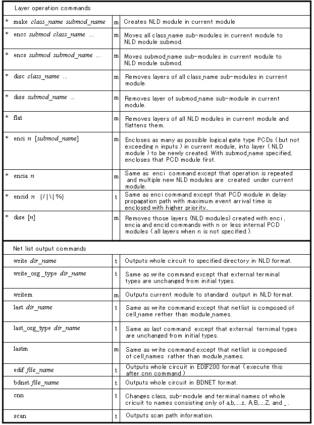
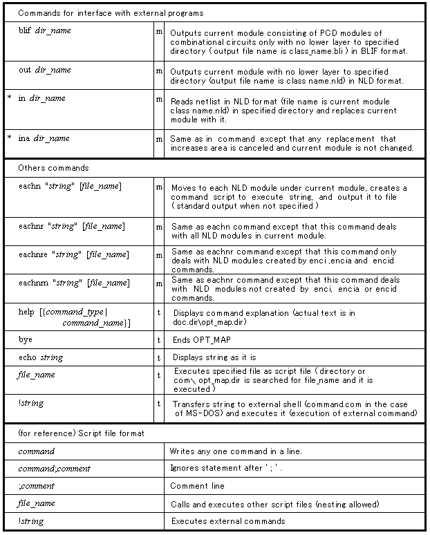
Table 7.1 provides a list of OPT_MAP commands. The details on each command can be displayed with the on-line help function which can be initiated by the 'help' command (MS-DOS's more.com is called from OPT_MAP).
<Table 7.1> List of OPT_MAP commands